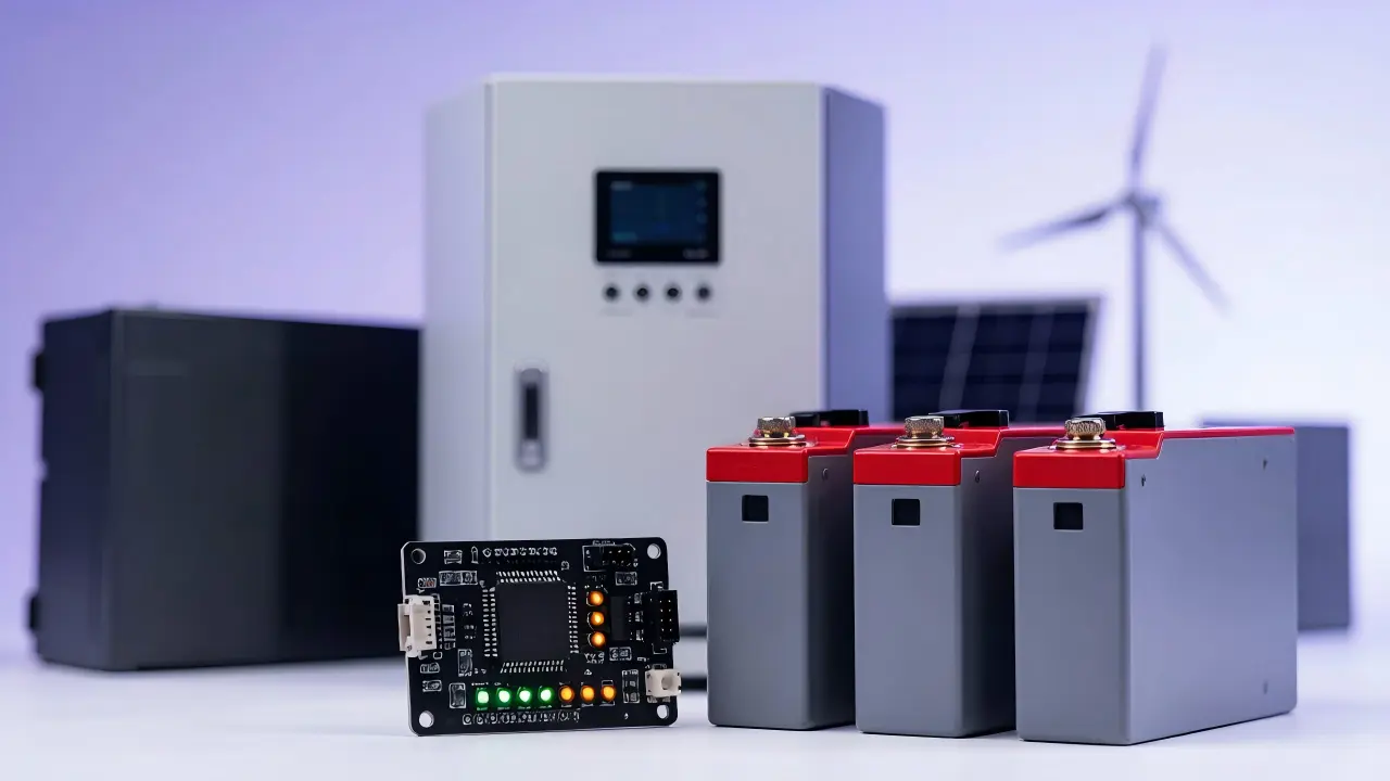

What Is a GaN Charger? How Gallium Nitride Beats Silicon
Published: September 2026
Reading time: 12 min
Audience: Buyers, product managers and technically curious readers who keep seeing “GaN” on charger boxes and want a plain-language answer to what is a GaN charger is, why it is smaller and cooler, and what it changes for OEM sourcing.
By Han — Paiyi Power, a Huizhou-based power supply OEM/ODM building GaN chargers and custom units 5W–240W, designed to USB PD 3.2 with SPR AVS. Buyers keep asking us one question — what is a GaN charger? — and this guide is our plain-language answer, from the material physics to the factory floor. We hold CE/CB/FCC/RoHS/ErP and ISO 9001, at MOQ 200 pcs per model.
Last updated: 29 September 2026.
Contents
Direct answer: what is a GaN charger?
What is a GaN charger? In one sentence: a power adapter whose main switching transistors are made of gallium nitride (GaN) — a wide-bandgap semiconductor — instead of the silicon MOSFETs inside conventional bricks. Because a GaN transistor switches faster and blocks higher voltage in a smaller die, everything magnetic around it shrinks too: a 65W GaN charger is typically about a third smaller than its silicon equivalent and wastes less energy as heat. The USB-C port, the cable and the USB PD negotiation work exactly as before. For a buyer, the practical meaning is simple — the same watt class in a smaller, cooler case, with the real differences living in density, efficiency and the engineering discipline behind the board.
The material science: why gallium nitride switches faster
Gallium nitride is a wide-bandgap semiconductor: its bandgap is roughly 3.4 electron-volts, versus about 1.1 eV for silicon. A wider bandgap means the material withstands a much stronger electric field before it breaks down — GaN’s critical field is about ten times silicon’s — so a GaN transistor can block high voltage in a far thinner layer of material. Thinner layers mean smaller dies with lower on-resistance. Electrons also move through GaN quickly: in the two-dimensional electron gas a GaN transistor uses, mobility is typically around 2,000 cm²/V·s, comfortably above silicon’s textbook value near 1,400 cm²/V·s. These are standard semiconductor figures, and they are the entire reason the category exists.
The practical payoff is switching speed. Because the device loses far less energy per transition, designers raise the switching frequency from the ~65–100 kHz a silicon flyback typically uses to several hundred kilohertz and beyond. Frequency is the master variable of adapter size: the higher it goes, the less energy the transformer and capacitors must store per cycle, so those components — and therefore the case — shrink. That is the physics in one line: GaN does not store less energy, it lets the circuit store it far more often in far smaller parts. The result is a charger that does the same job from a much smaller board.
GaN vs silicon chargers: what actually changes
So what actually changes when a charger moves from silicon to GaN? Not the watt rating on the label and not the PD negotiation — those stay the same. What changes is the physics budget: how much voltage the switch can block, how fast it can toggle, and how much waste heat each delivered watt costs. The table below compares the two materials on the properties that matter for chargers, using textbook-level values, and translates each into what a buyer actually notices at the desk.
| Property | Silicon | Gallium nitride | What it means for chargers |
|---|---|---|---|
| Bandgap | ~1.1 eV | ~3.4 eV | Higher field strength before breakdown, so smaller dies and magnetics |
| Electron mobility (typical) | ~1,400 cm²/V·s | ~2,000 cm²/V·s (2DEG) | Faster current flow supports quicker, cleaner switching |
| Switching frequency (typical) | ~65–100 kHz | Several hundred kHz to ~1 MHz | The main lever that shrinks the transformer and capacitors |
| Typical transformer size | Bulky, sized for low frequency | Roughly 2–3× smaller at the same power | The visible “smaller brick” buyers notice |
| Thermal behavior at 140W | More waste heat, larger cooling surfaces | Less heat per watt, tighter case | Runs cooler at load — if the board design is good |
Smaller, cooler, faster: the three buyer-visible benefits
Smaller. The higher switching frequency shrinks the transformer and the capacitors that dominate adapter volume, so a 65W GaN brick slips into a jacket pocket where a silicon unit would not. Cooler. Lower switching and conduction losses mean fewer watts burned as heat for the same output, which you can feel by holding both bricks after twenty minutes at full load. Faster is the third benefit, with a caveat: GaN does not make charging negotiate faster by itself. The speed you see comes from USB PD — the protocol, not the semiconductor — and from the device pulling what the port offers.
What GaN buys is headroom. The thermal and size savings let a design hold peak power longer without throttling, fit multi-port architectures that silicon cannot package, and still pass the temperature tests a safety file demands. For buyers, the three benefits stack into one sourcing argument: at equal watt class, GaN delivers the same job in a smaller, cooler case — provided the board around the chip is engineered and tested as seriously as the chip is made. The chip sets the ceiling; the design decides how much of it you get.
Inside a GaN charger: the board-level view
Open a GaN charger and the difference is architecture, not magic. The AC input is rectified as usual; the change happens on the power stage, where GaN FETs — discrete in simpler designs, or integrated with drivers and controllers in advanced ones — switch the DC bus into the transformer at high frequency. The secondary side rectifies and regulates the output, and a PD controller negotiates voltage with the device. Around those stages sit the parts that decide quality: a transformer wound for high frequency, the EMI filter that keeps the design legal, and a layout that keeps the fast-switching loops tight enough to stay quiet.
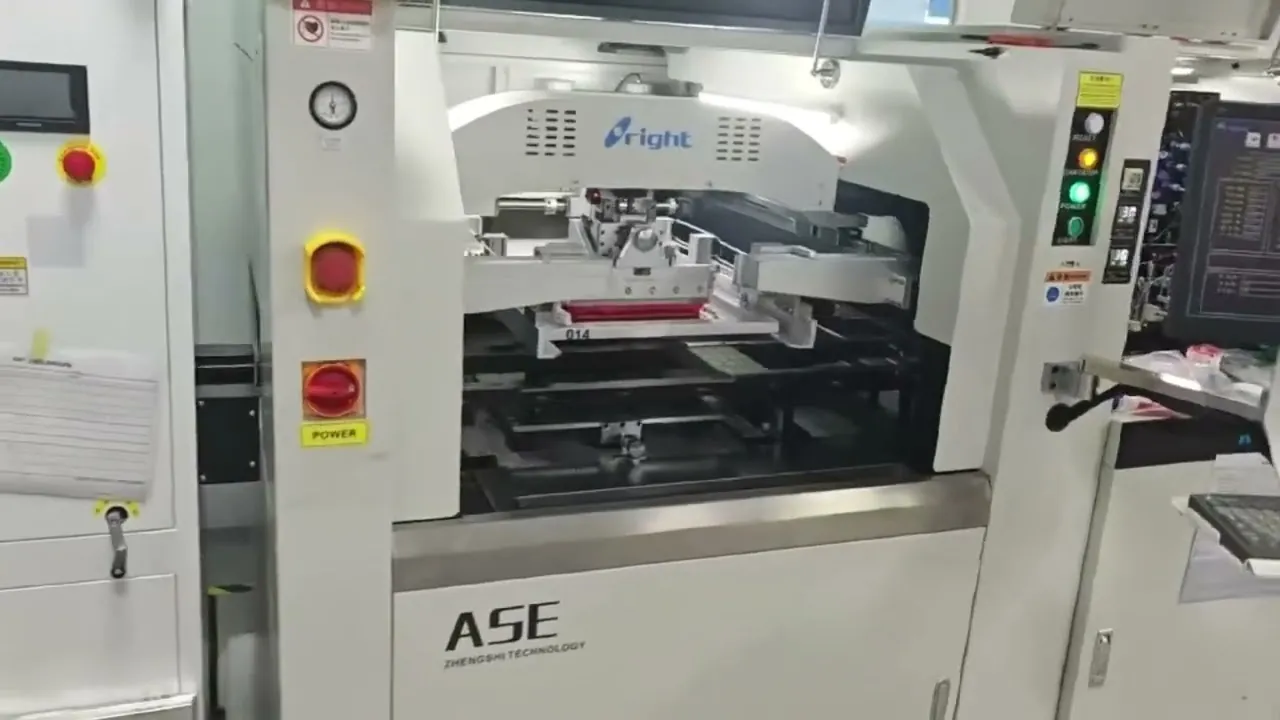
Production splits the same way. The PCBA is placed by SMT, then finished by hand — connectors, safety wiring, assembly and QC — before 100% functional test. For our GaN builds, placement runs at the Tier-1 SMT factory Paiyi Power holds a stake in (running Fuji NXT / M3S), and the boards return to Huizhou for incoming inspection, manual assembly, QC, ATE and burn-in. The die is commodity; the board and the process around it are not — which is exactly where an OEM earns or loses a buyer’s trust.
A short history: from lab curiosity to 140W bricks
GaN spent decades as a lab curiosity — LEDs and RF amplifiers — before power delivery made it commercial. The milestones below track how quickly the category moved from novelty to default, and what each step meant for buyers. The pattern is classic: every generation pushed the same watt class into a smaller case at a lower price, until GaN stopped being a premium option and became the expected way to build above 30W.
| Year | Milestone | Buyer impact |
|---|---|---|
| 2014 | First commercial GaN chargers ship | Early adopters paid a premium for travel-size power |
| 2017 | 27W consumer units reach the market | Phone makers adopt GaN for fast-charge bricks |
| 2019 | 65W becomes the mainstream sweet spot | One brick starts replacing laptop and phone chargers |
| 2021 | GaN spreads into 100W+ designs | Multi-port desktop charging goes compact |
| 2023 | 140W EPR bricks arrive | USB PD 3.1 EPR makes single-cable laptop power normal |
| 2026 | GaN 3 and the integration wave | Higher density and fewer parts at the same price tiers |
For an OEM buyer, that history is a planning tool rather than trivia. It shows which watt classes are mature — 65W is a solved problem with deep supplier bases — which are still premium, like 140W EPR builds that demand serious thermal and test rigor, and where the next cost-downs will come from, namely GaN 3 integration that folds drivers and controllers into the power stage. Matching a charger roadmap to that curve, and to protocol milestones such as EPR, keeps a program from launching against the grain of the supply base.
5 GaN myths buyers still believe
Myth one: “GaN” on the box is just marketing. The material’s advantage is measured physics — bandgap, critical field, switching loss — not a sticker. Myth two: a GaN chip guarantees a good charger. It does not; layout, transformer design, protection circuits and QC decide whether the physics reaches the port. Myth three: all GaN is the same. Integration tiers differ — discrete FETs versus half-bridge versus monolithic power stages — and the tier drives both price and failure modes.
Myth four: GaN runs cold, so thermal design can be relaxed. It runs cooler, not cold; a cramped 140W build can still cook itself, which is why burn-in and load testing matter as much as ever. Myth five: GaN automatically means certified. Certifications attach to the finished product against standards like IEC 62368-1, not to the semiconductor. A supplier who conflates the die with the certificate is telling you where their competence ends — listen.
Heat, efficiency and where the watts go
Efficiency decides where the watts go — or fail to go. Switching loss scales with frequency and conduction loss with current; GaN attacks the first, and its smaller, lower-resistance dies attack the second. At the same output, a well-designed GaN stage converts more of the wall’s energy into the device and less into the case, which is why a GaN brick at full load stays comfortable to hold where a comparable silicon unit becomes unpleasant. The saved heat is also design budget: it pays for the smaller case.
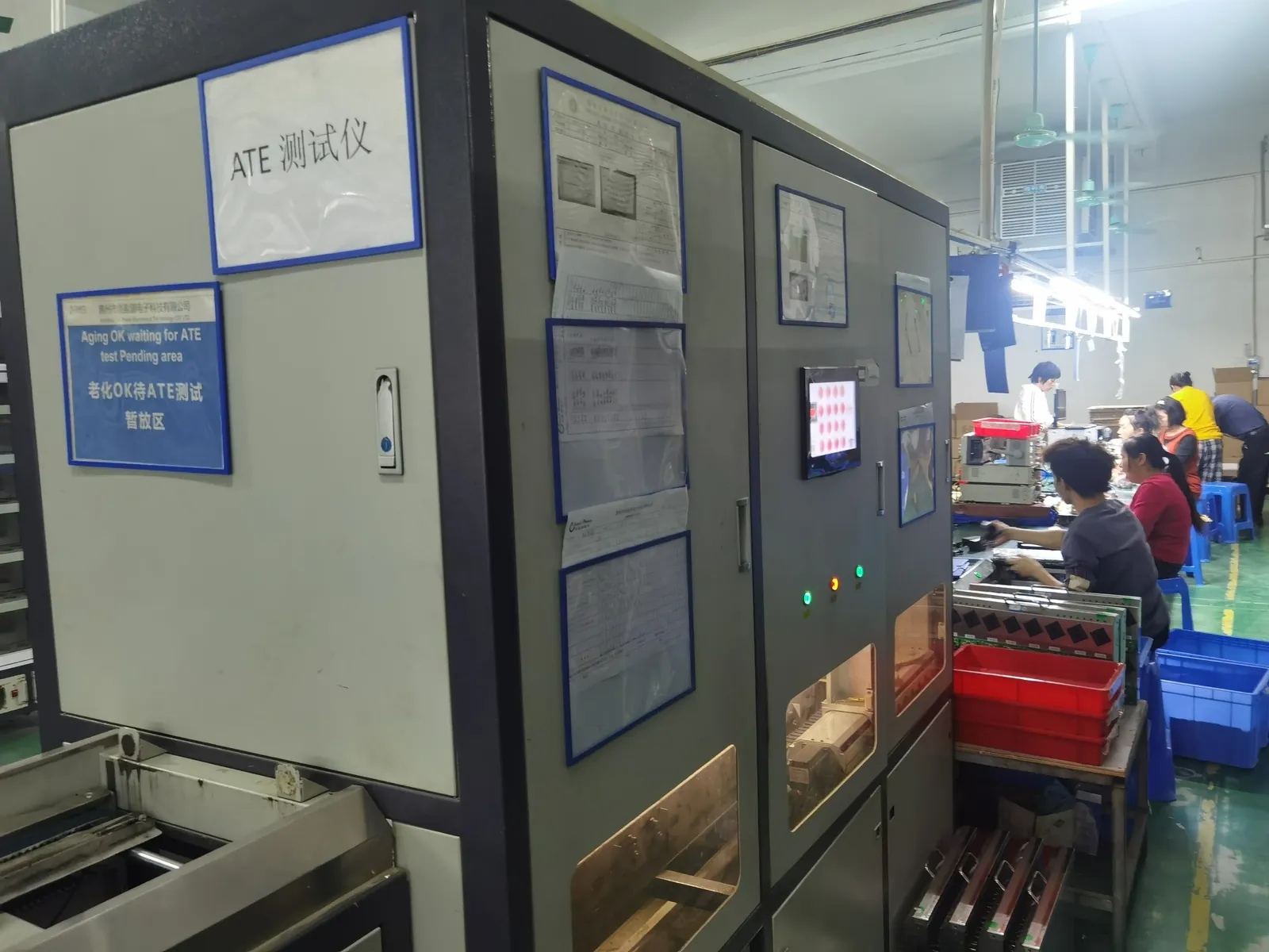
But a datasheet number is not a number at the port. Real efficiency depends on layout, transformer quality, component grades and assembly consistency — which is why a serious factory measures every unit rather than a sample. On our lines, each charger passes a 100% ATE functional test — output voltage and current, ripple, regulation, protection trips at the port — plus burn-in, so the efficiency claim survives contact with production. Ask any supplier how the figure you are quoted is verified; cable losses count too, which is where our voltage drop calculator earns its keep.
Does GaN matter at 20W? At 140W? It depends
Does GaN matter at every watt? No — and pretending otherwise is how buyers overpay. The benefit scales with how much the transformer and the thermal budget dominate the design, which is why the same material can be transformative at one watt class and marginal at another. The table below is the honest version: where GaN transforms the product, where it merely improves it, and what an OEM should weigh before committing a program to the material.
| Watt class | GaN benefit | How visible | OEM note |
|---|---|---|---|
| 20W | Modest size gain; silicon still competes on price | Visible (pocket bricks) | Cost-driven class; choose GaN only when size sells |
| 65W | Laptop and phone in one compact brick | Very visible in size and heat | The volume sweet spot for private label |
| 100W | Multi-port power without the bulk | Visible in dock and desktop use | EPR-capable design and QC depth matter more than the die |
| 140W | Full laptop load in a palm-size case | Highly visible; premium tier | PD 3.1 EPR plus tight thermal margins and full ATE coverage |
The rule of thumb: below roughly 30W, silicon and GaN cost structures overlap and the choice is often commercial; from 65W upward, GaN wins on size and heat in ways users feel; at 100W–140W with EPR, GaN is close to a requirement for meeting size expectations at the watt class. Pair the power-stage decision with the protocol one — our PD 3.1 vs PD 3.2 guide covers what EPR and AVS buyers should specify.
Why a GaN chip alone does not make a good charger
A GaN chip alone does not make a good charger, for the same reason an engine alone does not make a car. The die is among the least differentiating parts of a finished adapter; what separates a reliable brick from a returned one is everything wrapped around it: transformer quality, EMI design, protection circuits — over-voltage, over-current, over-temperature, short circuit — component grades, and the consistency of assembly. Two factories can buy the same GaN FET and ship chargers that behave very differently after six months in the field.
That is why process ownership matters more than the semiconductor. Manual assembly of safety-critical wiring, visual and functional QC, 100% ATE and burn-in are where reliability is actually manufactured. At Paiyi Power the PCBA returns from the partnered SMT line to Huizhou, where our own teams run assembly, QC, test and aging across four lines — the steps that decide field-failure rates are the steps we refuse to outsource. Buyers should weight suppliers by those owned steps, not by the chip brand on the bill of materials.

What is a GaN charger to an OEM buyer?
What is a GaN charger to an OEM buyer? Strip away the physics and it is a sourcing decision with three dials: watt class, port configuration and case size. GaN’s job is to make ambitious combinations buildable — 140W in a palm-size brick, three ports without a desk heater — but the dials interact: more ports demand smarter power allocation, smaller cases demand tighter thermal margins, and higher watt classes demand EPR-capable PD controllers and heavier test coverage.
Practically, the decision splits by tier. A 65W single-port private-label charger is table-stakes GaN, where the supplier’s process discipline is the real differentiator. A 100W+ multi-port build — see our 100W+ GaN charger OEM guide — turns on architecture choices and QC depth. At 140W, single versus multi-port changes the thermal problem entirely, so it deserves its own program; our 140W GaN charger supplier guide compares the two routes.
On mechanics, get numbers in writing: modified-standard builds start at MOQ 200 pcs per model, full custom ODM typically runs 500–1,000 pcs, sampling takes about 7 days on a modified standard and 2–4 weeks for full custom, and mass production runs 5–6 weeks after sample approval. A supplier who dodges those numbers is quoting enthusiasm, not capacity.
How to verify a supplier’s GaN competence
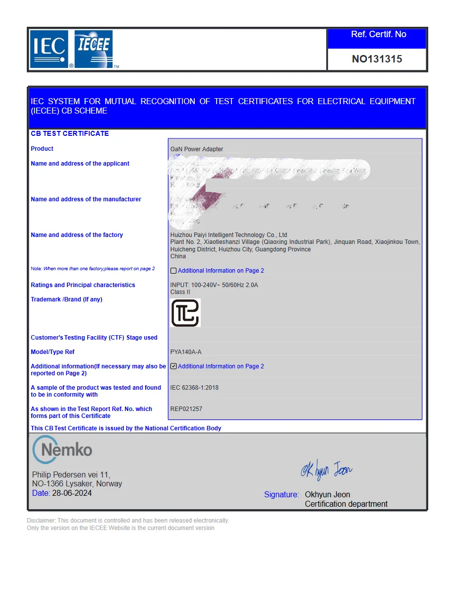
Verifying a supplier’s GaN competence is mostly verifying ordinary OEM discipline plus a few GaN-specific probes. Ask which GaN platform and integration tier they build on and what they have shipped at your watt class. Ask how the SMT step is controlled and what incoming inspection the PCBA passes. Then run the checks that apply to any power supply: ISO 9001 certification, model-specific certificates — CE, CB under IECEE, FCC, RoHS, ErP — a frozen BOM, defined test limits, and 100% final inspection with ATE and burn-in you can watch running.
The certificate check deserves special emphasis, because certifications attach to the finished model, not the semiconductor. Demand the PDF for your exact watt class — a 140W PD 3.2 build should come with a CB certificate you can read, not a family cert for another product. UL/ETL/UKCA and similar national marks are buyer-funded on most OEM programs; a factory that claims them unprompted is overclaiming. Use our GaN charger manufacturer checklist to structure the visit, and treat one evasive answer as the answer.
GaN 3, integration and what comes next
Three currents define where GaN charging goes next. First, integration: newer GaN generations fold drivers, controllers and protection into the power stage itself, cutting part count and the failure modes that come with it. Second, power over USB-C: PD 3.1 EPR at 140W is now mainstream for laptops, with adjustable-voltage rails that silicon-era designs never had to negotiate. Third, density: every generation fits the same watts into a smaller case at a lower cost, and GaN 3 continues that curve.
For buyers, the near future looks like consolidation more than revolution: fewer, smarter GaN chargers covering whole device fleets, with firmware-adjustable behavior and tighter integration between cable, brick and device. The sourcing implication survives all of it unchanged — the winning suppliers will be those whose process, test and certification discipline keep pace with the silicon, because the chip improves on a roadmap while quality only improves on the floor. Our custom power supply manufacturer guide covers how that collaboration runs from brief to bulk shipment.
Frequently asked questions
These are the GaN charger questions buyers ask most, answered without the sales gloss.
What is a GaN charger in one sentence?
A GaN charger is a power adapter whose main switching transistors are made of gallium nitride instead of silicon, which lets the design switch at much higher frequency, use a smaller transformer and waste less energy as heat. The result is the same watt class in a smaller, cooler case — a 65W GaN brick is typically about a third smaller than its silicon equivalent. Ports, cables and USB PD negotiation work exactly as before; the difference is physics, not protocol.
Is GaN really better than silicon?
Yes, on the properties that matter for chargers: GaN’s bandgap is about 3.4 eV versus silicon’s 1.1 eV, it withstands roughly ten times the electric field, and it switches with lower loss at the frequencies adapters use. That converts directly into smaller size and less heat at the same watt class. The honest caveat: a good silicon charger outperforms a badly designed GaN one, because the chip is only part of the product — layout, protection and QC decide the rest.
Why are GaN chargers smaller?
Size in an adapter is set by how much energy the transformer and capacitors must store per switching cycle. GaN transistors switch far faster with lower losses, so designers raise the switching frequency from the ~65–100 kHz typical of silicon flybacks to several hundred kilohertz or more. Each cycle stores less energy, so the magnetic and capacitive parts shrink — and they are the bulk of the case. Higher frequency is the mechanism; smaller is the consequence.
Do GaN chargers run cooler?
Usually yes, at the same watt class. Lower switching and conduction losses mean fewer watts burned inside the case for the same output, so both the case and the device being charged stay cooler under load. The gain is real but not automatic: a cramped layout, a cheap transformer or skipped burn-in can erase it. Judge cooling by measured case temperature at full load on the finished unit, not by the semiconductor on the bill of materials.
Are GaN chargers safe?
A properly built one, yes — safety comes from the finished product meeting standards such as IEC 62368-1, not from the semiconductor itself. A competent OEM designs in protection (over-voltage, over-current, over-temperature, short circuit), verifies isolation with hipot testing on 100% of units, and holds model-specific certificates: CE, CB under IECEE, FCC, RoHS and ErP. The risk sits with suppliers who treat GaN as a marketing layer without the process behind it, which is exactly what an audit is for.
Does GaN matter for low-watt chargers?
Less than at higher watt classes. At 20W, silicon designs are cheap, compact and mature, so GaN’s advantage shrinks to a modest size gain at a price premium many buyers will not pay. The physics still applies, but the transformer is already small and the thermal margin comfortable. Where it starts to matter is roughly 65W and up, where the magnetic components dominate and the heat at full load becomes something the user notices.
What is a GaN charger’s lifespan?
A well-built GaN charger should last as long as a good silicon one — several years of daily use, typically engineered around electrolytic capacitor life and thermal stress. GaN itself switches with lower loss, which helps, but the capacitors and the transformer remain the aging parts. What predicts lifespan is not the semiconductor but the build: component grades, thermal design, 100% testing and burn-in at the factory. Ask a supplier how they verify aging, not which die they use.
Why are some GaN chargers cheap and others expensive?
Because the chip is a small share of the cost. Price tracks the integration tier of the GaN solution, the transformer and component grades, protection completeness, certification coverage, and how much testing each unit receives. A cheap build usually samples its safety tests, uses a family certificate and skips burn-in; a better one tests 100% of units and documents it. You are rarely paying for the GaN — you are paying for the process around it.
What should buyers check before ordering GaN chargers?
The same discipline as any OEM power supply, plus GaN-specific questions: the supplier’s watt-class track record, who controls the SMT step and what incoming inspection the PCBA passes, a frozen BOM with defined test limits, 100% ATE plus burn-in, and model-specific certificates (CE, CB, FCC, RoHS, ErP) rather than vague claims. Confirm the PD specification — designed to USB PD 3.2 specification (with SPR AVS) is the current baseline — and MOQ, sampling time and mass-production lead time in writing.
Sources
- Wikipedia — Gallium nitride (wide-bandgap semiconductor)
- USB Implementers Forum — USB Power Delivery specification
- Energy Star — External Power Supplies program
- IEC — IEC 62368-1 (audio/video/ICT equipment safety)
- IECEE — CB Scheme (global certification for electrical equipment)
Related reading
- 100W+ GaN charger OEM: the complete selection guide
- 140W GaN charger supplier: single vs multi-port guide
- PD 3.1 vs PD 3.2: what EPR and AVS buyers should choose
- How to vet a GaN charger manufacturer: 12-point checklist
- Custom power supply manufacturer: the complete OEM process guide
- White label GaN charger vs ODM: 5 levels of customization